SMART researchers create world’s smallest LED and holographic microscope that enable conversion of existing mobile phone cameras into high-resolution microscopes
Singapore researchers at SMART have developed the world’s smallest silicon (Si) light-emitting diode (LED) coupled with state-of-the-art Si LEDs and with multiple potential applications. The invention enables to reconstruct objects measured by this microscope, including plant seeds and tissue samples – enabling enhanced microscopic examination of a wide range of objects that has been impossible previously, as well as the detection of plant disease and aberrant plant tissues.
Researchers from the e Disruptive & Sustainable Technologies for Agricultural Precision (DiSTAP) and the Critical Analytics for Manufacturing Personalized-Medicine (CAMP) Interdisciplinary Research Groups (IRG) of Singapore-MIT Alliance for Research and Technology (SMART), MIT’s research enterprise in Singapore.
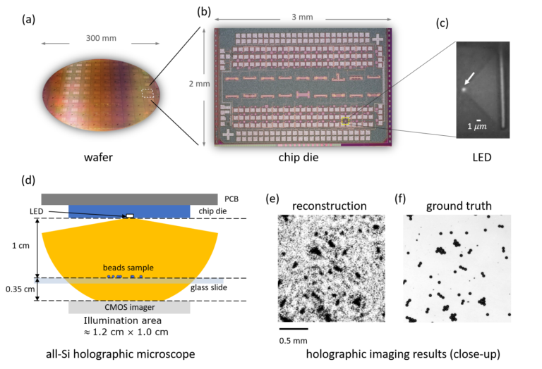
The new world’s smallest LED (light emitting diode) enables the conversion of existing mobile phone cameras into high-resolution microscopes. Smaller than the wavelength of light, the revolutionary LED was used to build the world’s smallest holographic microscope, paving the way for existing cameras in everyday devices such as mobile phones to be converted into microscopes via only modifications to the silicon chip and software. This technology also represents a significant step forward in the miniaturization of diagnostics for indoor farmers and sustainable agriculture.
This breakthrough was supplemented by the researchers’ development of a revolutionary neural networking algorithm that reconstructs objects measured by the holographic microscope. This enables enhanced examination of microscopic objects such as cells and bacteria without bulky conventional microscopes or additional optics. The research also paved the way for a major advancement in photonics – the building of a powerful on-chip emitter smaller than a micrometer, which has long been a challenge in the field.
The novel LED developed by SMART researchers is a CMOS-integrated sub-wavelength scale LED at room temperature exhibiting high spatial intensity (102 ± 48 mW/cm2) and possessing the smallest emission area (0.09 ± 0.04 μm2) among all known Si emitters in scientific literature. In order to demonstrate a potential practical application, the researchers incorporated this LED into an in-line, centimeter-scale, all-silicon holographic microscope requiring no lens or pinhole, integral to a field known as lensless holography. The research team also developed a deep neural network architecture to improve the quality of image reconstruction.
The researchers envision that this synergetic combination of CMOS micro-LEDs and the neural network can be used in other computational imaging applications, such as a compact microscope for live-cell tracking or spectroscopic imaging of biological tissues such as living plants. This work also demonstrates the feasibility of next-generation on-chip imaging systems. Already, in-line holography microscopes have been employed for a variety of applications, including particle tracking, environmental monitoring, biological sample imaging, and metrology. Further applications include arraying these LEDs in CMOS to generate programmable coherent illumination for more complex systems in the future.

